基于FPGA的CNN卷积神经网络设计指南
目录
2.6 Batch Normalization层原理与FPGA实现
随着人工智能技术的飞速发展,深度学习和强化学习已经在图像识别、自然语言处理、自动驾驶、机器人控制等领域取得了突破性进展。然而,传统的GPU和CPU平台在部署这些模型时,往往面临功耗高、延迟大、体积大等问题,难以满足边缘计算和实时推理的需求。FPGA凭借其高度并行的计算架构、可重构性、低功耗和低延迟等优势,成为部署AI模型的理想硬件平台。本文将以卷积神经网络(CNN)作为深度学习的例阐述如何在FPGA上实现CNN模型。
1.FPGA定点运算
在FPGA中,浮点运算消耗大量资源,因此通常采用定点数表示。例如,使用16位定点数,其中1位符号位、7位整数位、8位小数位(Q7.8格式):
![]()
Verilog中,定点数直接用有符号寄存器表示:
// 定点数定义:16位,Q7.8格式
// 符号位1位 + 整数部分7位 + 小数部分8位
reg signed [15:0] fixed_point_value;

// 定点数乘法:两个Q7.8数相乘后需右移8位截断
module fixed_multiply (
    input  signed [15:0] a,      // Q7.8
    input  signed [15:0] b,      // Q7.8
    output signed [15:0] result  // Q7.8
);
    wire signed [31:0] mult_full;
    assign mult_full = a * b;           // 32位全精度结果
    assign result = mult_full[23:8];    // 右移8位,取回Q7.8格式
endmodule
定点数加法相对简单,同格式的定点数可直接相加:
![]()
Verilog如下:
module fixed_add (
    input  signed [15:0] a,
    input  signed [15:0] b,
    output signed [15:0] result
);
    wire signed [16:0] sum_full;
    assign sum_full = a + b;
    // 饱和处理,防止溢出
    assign result = (sum_full > 17'sd32767)  ? 16'sd32767 :
                    (sum_full < -17'sd32768) ? -16'sd32768 :
                    sum_full[15:0];
endmodule
2.卷积神经网络的FPGA实现
卷积神经网络是深度学习中最经典的网络架构之一,广泛应用于图像分类、目标检测等任务。一个典型的CNN包含以下层次:卷积层(Convolution Layer)、激活函数层(Activation Layer)、池化层(Pooling Layer)和全连接层(Fully Connected Layer)。
整个系统的流程图如下图所示:
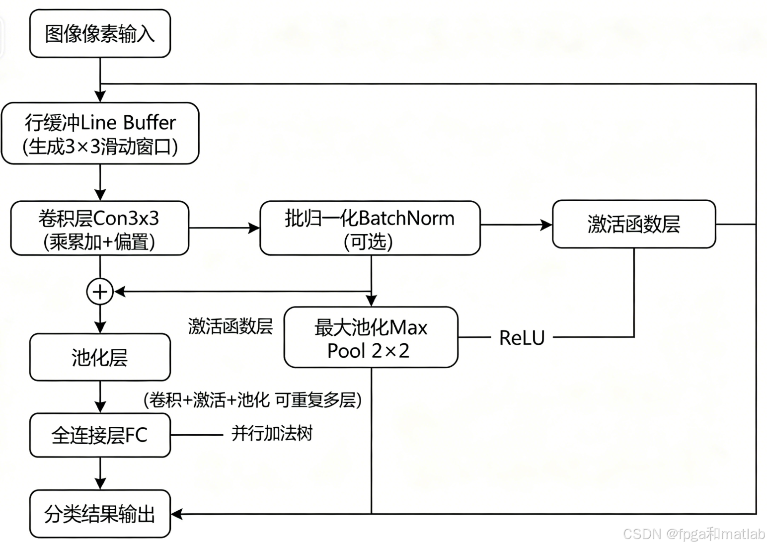
2.1 卷积层原理与FPGA实现
卷积层是CNN的核心运算。对于二维卷积,设输入特征图为I,卷积核为K,输出特征图为O,偏置为b,则卷积运算定义为:
![]()
其中,Kh和Kw分别是卷积核的高度和宽度。对于多通道情况,假设输入有Cin个通道,输出有 Cout个通道,则:
![]()
以最常见的3×3卷积核为例,实现单通道卷积运算。卷积本质上是乘累加操作:
module conv3x3 (
    input  wire        clk,
    input  wire        rst_n,
    input  wire        valid_in,
    // 3x3输入窗口数据(Q7.8定点数)
    input  signed [15:0] pixel_00, pixel_01, pixel_02,
    input  signed [15:0] pixel_10, pixel_11, pixel_12,
    input  signed [15:0] pixel_20, pixel_21, pixel_22,
    // 3x3卷积核权重(Q7.8定点数)
    input  signed [15:0] weight_00, weight_01, weight_02,
    input  signed [15:0] weight_10, weight_11, weight_12,
    input  signed [15:0] weight_20, weight_21, weight_22,
    // 偏置
    input  signed [15:0] bias,
    // 输出
    output reg signed [15:0] conv_out,
    output reg         valid_out
);

    // 乘法结果(32位全精度)
    wire signed [31:0] mult [0:8];

    // 9个并行乘法器
    assign mult[0] = pixel_00 * weight_00;
    assign mult[1] = pixel_01 * weight_01;
    assign mult[2] = pixel_02 * weight_02;
    assign mult[3] = pixel_10 * weight_10;
    assign mult[4] = pixel_11 * weight_11;
    assign mult[5] = pixel_12 * weight_12;
    assign mult[6] = pixel_20 * weight_20;
    assign mult[7] = pixel_21 * weight_21;
    assign mult[8] = pixel_22 * weight_22;

    // 加法树结构实现累加(流水线第一级)
    wire signed [31:0] sum_level1 [0:3];
    assign sum_level1[0] = mult[0] + mult[1];
    assign sum_level1[1] = mult[2] + mult[3];
    assign sum_level1[2] = mult[4] + mult[5];
    assign sum_level1[3] = mult[6] + mult[7];

    // 加法树第二级
    wire signed [31:0] sum_level2 [0:1];
    assign sum_level2[0] = sum_level1[0] + sum_level1[1];
    assign sum_level2[1] = sum_level1[2] + sum_level1[3];

    // 加法树第三级
    wire signed [31:0] sum_level3;
    assign sum_level3 = sum_level2[0] + sum_level2[1];

    // 最终累加:加上第9个乘法结果和偏置
    wire signed [31:0] sum_final;
    assign sum_final = sum_level3 + mult[8] + (bias <<< 8); // 偏置对齐到Q14.16

    // 截断回Q7.8格式,并进行饱和处理
    wire signed [15:0] result_truncated;
    assign result_truncated = sum_final[23:8];

    always @(posedge clk or negedge rst_n) begin
        if (!rst_n) begin
            conv_out  <= 16'd0;
            valid_out <= 1'b0;
        end else begin
            conv_out  <= result_truncated;
            valid_out <= valid_in;
        end
    end

endmodule
2.2 激活函数层原理与FPGA实现
ReLU是最常用的激活函数,其数学表达式为:
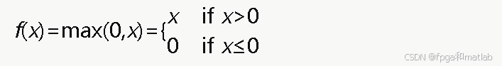
ReLU函数在FPGA上实现极为高效,只需要检查符号位即可。
程序如下:
module relu (
    input  wire signed [15:0] data_in,
    output wire signed [15:0] data_out
);
    // 当符号位为1(负数)时输出0,否则输出原值
    assign data_out = data_in[15] ? 16'd0 : data_in;
endmodule
2.3 Sigmoid函数的分段线性近似与FPGA实现
Sigmoid函数定义为:
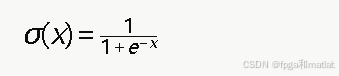
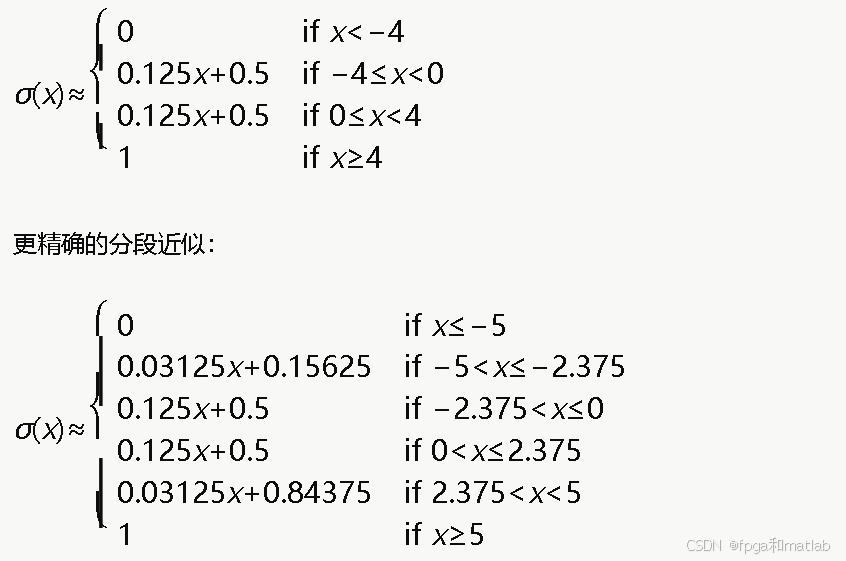
由于Sigmoid涉及指数运算和除法,在FPGA上直接实现非常复杂。常用的方法是分段线性近似:
程序如下:
module sigmoid_pwl (
    input  wire signed [15:0] data_in,   // Q7.8
    output reg  signed [15:0] data_out   // Q7.8, 输出范围[0,1]
);
    // 常数定义(Q7.8格式)
    localparam signed [15:0] NEG5     = -16'sd1280;  // -5.0 * 256
    localparam signed [15:0] NEG2_375 = -16'sd608;   // -2.375 * 256
    localparam signed [15:0] POS2_375 =  16'sd608;
    localparam signed [15:0] POS5     =  16'sd1280;
    localparam signed [15:0] ONE      =  16'sd256;   // 1.0 * 256
    localparam signed [15:0] HALF     =  16'sd128;   // 0.5 * 256

    wire signed [31:0] mult_result;

    always @(*) begin
        if (data_in <= NEG5) begin
            data_out = 16'd0;
        end else if (data_in <= NEG2_375) begin
            // 0.03125 * x + 0.15625
            // 0.03125 = 8 in Q7.8, 0.15625 = 40 in Q7.8
            data_out = ((data_in * 16'sd8) >>> 8) + 16'sd40;
        end else if (data_in <= POS2_375) begin
            // 0.125 * x + 0.5
            // 0.125 = 32 in Q7.8, 0.5 = 128 in Q7.8
            data_out = ((data_in * 16'sd32) >>> 8) + HALF;
        end else if (data_in < POS5) begin
            // 0.03125 * x + 0.84375
            // 0.84375 = 216 in Q7.8
            data_out = ((data_in * 16'sd8) >>> 8) + 16'sd216;
        end else begin
            data_out = ONE;
        end
    end
endmodule
2.4 最大池化层原理与FPGA实现
最大池化对每个池化窗口取最大值,以2×2窗口、步长为2为例:

最大池化能够保留区域内最显著的特征,同时将特征图尺寸缩小为原来的一半。
最大池化的Verilog实现如下:
module max_pool_2x2 (
    input  wire signed [15:0] pixel_00,
    input  wire signed [15:0] pixel_01,
    input  wire signed [15:0] pixel_10,
    input  wire signed [15:0] pixel_11,
    output wire signed [15:0] pool_out
);
    wire signed [15:0] max_row0, max_row1;

    // 第一行取最大值
    assign max_row0 = (pixel_00 > pixel_01) ? pixel_00 : pixel_01;
    // 第二行取最大值
    assign max_row1 = (pixel_10 > pixel_11) ? pixel_10 : pixel_11;
    // 两行结果再取最大值
    assign pool_out = (max_row0 > max_row1) ? max_row0 : max_row1;

endmodule
2.5 全连接层原理与FPGA实现
全连接层本质上是矩阵向量乘法加偏置:
![]()
其中x是输入向量(长度为N),w是权重矩阵,b是偏置向量,y是输出向量。
以一个输入维度为4、输出维度为1的简单全连接神经元为例:
module fully_connected #(
    parameter INPUT_DIM = 4
)(
    input  wire        clk,
    input  wire        rst_n,
    input  wire        start,
    input  wire signed [15:0] x [0:INPUT_DIM-1],  // 输入向量
    input  wire signed [15:0] w [0:INPUT_DIM-1],  // 权重向量
    input  wire signed [15:0] bias,                 // 偏置
    output reg  signed [15:0] y,                    // 输出
    output reg         done
);

    reg [2:0] state;
    reg [15:0] idx;
    reg signed [31:0] acc;  // 累加器

    localparam IDLE    = 3'd0;
    localparam COMPUTE = 3'd1;
    localparam OUTPUT  = 3'd2;

    always @(posedge clk or negedge rst_n) begin
        if (!rst_n) begin
            state <= IDLE;
            acc   <= 0;
            y     <= 0;
            done  <= 0;
            idx   <= 0;
        end else begin
            case (state)
                IDLE: begin
                    done <= 0;
                    if (start) begin
                        acc   <= 0;
                        idx   <= 0;
                        state <= COMPUTE;
                    end
                end

                COMPUTE: begin
                    // 乘累加:acc += x[idx] * w[idx]
                    acc <= acc + (x[idx] * w[idx]);
                    if (idx == INPUT_DIM - 1) begin
                        state <= OUTPUT;
                    end else begin
                        idx <= idx + 1;
                    end
                end

                OUTPUT: begin
                    // 加偏置并截断
                    y    <= (acc + (bias <<< 8)) >>> 8;
                    done <= 1;
                    state <= IDLE;
                end
            endcase
        end
    end

endmodule
2.6 Batch Normalization层原理与FPGA实现
Batch Normalization(批归一化)在推理时可简化为线性变换:

其中,γ^和 β^在训练完成后是固定常数,因此在FPGA推理中只需实现一次乘加运算。
Verilog实现如下:
module batch_norm (
    input  wire signed [15:0] data_in,
    input  wire signed [15:0] gamma_hat,  // 预计算的缩放因子
    input  wire signed [15:0] beta_hat,   // 预计算的偏移量
    output wire signed [15:0] data_out
);
    wire signed [31:0] scaled;
    assign scaled = data_in * gamma_hat;
    assign data_out = scaled[23:8] + beta_hat;
endmodule

AtomGit 是由开放原子开源基金会联合 CSDN 等生态伙伴共同推出的新一代开源与人工智能协作平台。平台坚持“开放、中立、公益”的理念,把代码托管、模型共享、数据集托管、智能体开发体验和算力服务整合在一起,为开发者提供从开发、训练到部署的一站式体验。
更多推荐


 10
10 0
0- 0


 已为社区贡献22条内容

所有评论(0)